switch mode power supply design your primary source for creative solutions
Introduction
Our design experience in power electronics started 1992 with the design of a small Switch Mode Power Supply featuring an extremely wide input range from 24V till 240V DC/AC.
Since then, a broad range of designs were created, not only SMPS, but also lighting power converters and industrial motor controllers. The year 2013 marks a specialisation towards these areas. Originally, our electronics engineering was of generic nature. The focusing allows us to carry out more challenging designs.
Today, our thorough understanding of circuits and importantly also of precise EMI sources in a practical design helps in reaching the goals you expect without time consuming trial & error processes. As such, expensive overkill in EMI-suppression measures is avoided.
Please note that this overview - recent work on top - is of quite technical nature. Highlighted text supports a quick query of notable design aspects resp. technical issues.
projects since 2013
Expertise consultations
A class of servicing customer needs beyond systems development has been carried out for two business units of a new global customer (2021): EMC-related consultation of two different industrial power supplies in the power range of approx. 200 W where measures should be identified in order to achieve household norms instead of industry class EMC norms. Extensive experiments resulted in a range of proposed measures, where it’s up to the developer firm to make a selection.
A second consultation had the focus of finding the root cause of failure in recent production batches of small, few Watts SMPS units. The root cause appeared to be within the bought-in transformer. Microscopic analysis proved this.
In both cases, former consultations by other third parties were without success. This inspired us to add a slogan on our introduction page: You can count on us.
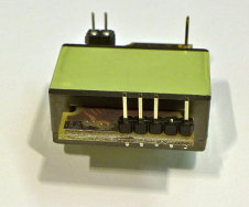
Innovative Planar Transformer based power supply
The design and prototyping of planar transformer technology for usage in very low profile SELV equipment, operated on mains voltage, represents a cutting-edge technology work for us. This project includes the design of the switch mode power supply circuit as well. Here, a novel single-stage half bridge approach with PFC has been utilized operating on a fixed frequency and a passive secondary side as well. Output voltage is regulated using Primary Side Control by modulating the duty cycle via PWM drive of the half bridge. Even a sophisticated PFC-operation with secondary side bulk capacitor is part of the design. Its advantage is the lack of a huge inrush current.
The fixed frequency helps reduce the effort to achieve full EMC-compatibility. For example QR-flyback topologies as well as LLC topologies suffer of a wide PWM frequency operating range which may result in violation of switching noise limits in the 150-800 kHz range (line input), when some harmonics are peaking upon very certain power levels delivered to the output. Of course, the switching frequency (here approx. 350 kHz) includes some jitter in order to allow smaller filter components to being used, and hence, cut costs.
prototype (h = 9.3 mm)
The topology makes resonant techniques superfluous because no snubber networks are necessary. Efficiency levels reach beyond 91 % (in PFC-operation), with the perspective of further improvements. The transformer’s ferrite core has a footprint of 23x14 mm (see images) and a height of 8 mm, and is designed to
deliver 33 W to the DC output (with 100 Hz ripple voltage, magnitude dependent on bulk cap size). The transformer design has been approved by VDE, and could be customized towards a lower profile or higher power levels.
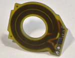
current density simulation
Specific requirement was a total height of the electronics of below 12 mm and approx. 24x220 mm footprint. It is not that common to construct a mains powered planar transformer in this power class because the insulation distances required according to EN 61558 are absolute. Smaller transformers have thus less space left over for windings.
Electronic LED Ballast design improvements (revisited)
The same project as described below has been optimized once again because of unit temperature and output power derating as well as EMI-problems arising with specific application geometry/enclosure conditions. This time, the customer could be convinced that the boost till 20 W output power could only reliably be reached by a transformer redesign. So this had been executed, together with necessary adjustments in the circuit (2017). Later, a further power boost step till 24 W has been realised, too: With another transformer change only intended for one specific load with higher output voltage and same maximum current (2020).
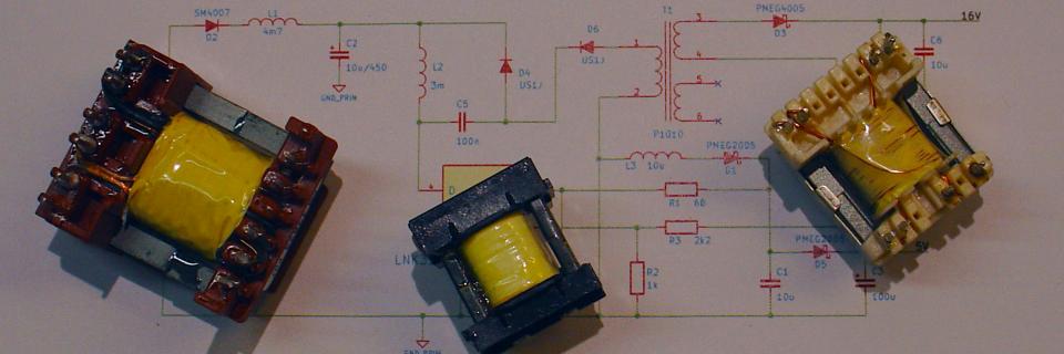
extremely wide input range SMPS
The first project at all (1992) “meets this project” (refer to the page’s end). In a nutshell: two cascaded conversion stages allow an extremely wide input range because the intermediate voltage range between the stages is a square root of the input voltage range. Hence the duty cycle varies much less on input voltage changes. In the former case, two separate MOSFETs do the switching. In this case, only one MOSFET is used (2017, in progress).
If non-isolated low voltage (as well as an isolated) output is desired, this cascaded concept is quite advantegeous:
The non isolated output can well be as low as 5V, also when AC input reaches beyond 300V. Modern tiny mains fed buck converters should not be designed for an output voltage lower than approx. 12V (very low Duty Cycle).
Despite being flyback nature (MOSFET switching to GND), snubber networks aren’t needed.
SMPS with metering till 480V AC
After successful finishing of the metering SMPS project as described in overnext section, the end customer ordered the development of a follow-up product designed with SMPS not reaching till 277VAC but till 480VAC (+10%). It was decided to use a modified version of the 440V PSR-design as described in the next section (PSR: see optocoupler free SMPS). A new primary side snubber network approach was utilized here in order to minimize the voltage peak (because of the 480V requirement), without more snubber losses - even contrary: less losses.
The first prototype iteration operated as expected. Only a dumb error in reasoning while swapping a filter element in order to ease the layouter’s work (affects EMI solely because of metering circuitry) made it necessary to enter a second prototype iteration.
Finally, high customer satisfaction could be reached, partly because of very good line and load regulation of the metering and the isolated low voltage supply for a bunch of connectivity functions and other stuff (2016-2017).
In a meeting, the end customer attested us high SMPS expertise.
metering SMPS redesign
The SMPS part of a three phase metering device in close proximity to 400/440V power distribution switches was subject to redesign because the end customer requested norm conformity to the household (B) norm instead of industrial (A) norm. Since the customer didn’t succeed in reaching this, we were engaged (2016).
The transformer has been redesigned with far higher primary inductivity (while ignoring advices some experts gave the customer before) and some layer details have been changed. Further, the layouter was instructed to do some assignment and placement changes in order to allow minimized coupling effects of high voltage switching to e.g. the input circuitry.
Further, the EMI suppression components had to be redesigned, and a tough EMI difficulty related to the metering GND coupling to Line (user selectable to Neutral or L2) could be solved as well.
Big effort was taken to replace the input DC bus capacitor by a smaller one, by simply allowing a far higher ripple voltage. Ambient temperatures up to 95°C were a tough requirement. The pre-existing DC-link film capacitor could only hardly be replaced by a far smaller one. Here, we extensively learnt how-to details regarding lifetime (FIT) computations with filmcaps and elcaps.
EMI problems solving
In a crucial project phase of a metering application for streetlight units where EMI problems seemed unresolvable, we were asked to analyse the problems. Just as an illustration of the complexity: a common mode choke may not work as expected, because a low voltage output GND of the transformer must be coupled directly to Neutral (metering circuit), and thus a noise voltage is injected in Line. One of the measures in this case was transferring the common mode choke to the secondary output that’s connected to the outside world (2016).
The transformer was improved on our suggestions, too, as well as some other EMI-related filtering details.
Another product, a lighting controller with DALI master, suffered of either EMI too high on the mains side or on the DALI side (one could speak of “balancing” the EMI output on both sides of the transformer). Here, a design modification of transformer as well as layout changes helped in meeting EMI requirements with 6 dB margin to norms (2016).
Electronic LED Ballast design
The SMPS part of a new 40W ballast was designed from the ground up as a two stage design: A PFC followed by a flyback converter (2014-2015).
In order to meet EMI requirements with inexpensive filter components, a simple passive network was added to the secondary side to neutralize the parasitic voltage over the transformer’s primary-secondary boundary.
EMI problems
A secondary side LED controller (not part of our efforts) exhibited EMI problems in approx. 60-80 MHz range. MOSFETS as part of a synchronous buck regulator (0-50V) showed to have too steep switching slopes while propagation delay was only moderate (this combination is prone to ringing or even oscillation problems). Another MOSFET was selected instead as well as the gate was loaded with extra capacitance. Further, layout changes were proposed and some SMD ferrite decoupling was modified.
Another secondary side buck converter for the board ‘logic’ suffered of being operated in burst mode even in normal operating conditions. The burst frequency even affected the operation of the main 40W SMPS. Here too, some design and layout changes were adviced.
Electronic LED Ballast design improvements
An existing design has been improved in terms of standby power consumption, EMI, power-on time and DC-mains detection (2013). Further, an output power increase from 15-20W was engineered (2014).
EMI problems
Strange, difficult to localize EMI problems in production samples were found to be caused by manufacturing failures of the common-mode input choke. The choke manufacturer consented to recourse claims, partially related to an unknown amount of units already out there. The customer was highly grateful with the investigation and its outcome.
Settop-box supply
A SEPIC topology was realised in order to convert a power cord 5-24V input supply to 5V. The circuit contains a Li-Ion cell with charger and a MOSFET switch to connect the Li-Ion cell to the SEPIC input when external power is off (2013).
Of course the charger is disabled when the cell is powering the application, in order to prevent a loop where the cell charges itself 😉.
Former projects
PoE power supply
(2009) See description near the page bottom (two isolation boundaries SMPS).
46V/250W boost converter with quasi-PFC
In an existing linear robot, the DC supply of up to three Maxon motor controllers was established via a conventional mains toroid core transformer, bridge rectifier and bulk capacitors. This arrangement suffered of limited peak power due to a high crest factor.
A better agility of motor stop & go without complete supply redesign was established by inserting a PFC boost converter between rectifier and bulk capacitors (2007). Standard boost converters for low voltage do not offer PFC behaviour. Instead, by modifications of the feedback loop, acceptable PFC-like behaviour was achieved, such that transformer utilization could be improved, resulting in following improvements:
more peak power for motor acceleration due to higher bus voltage (more capacitor energy dragging possible)
defined DC bus voltage independent of mains deviations
defined difference between max. voltage and bus voltage allows more break energy storage in the bulk capacitors
increase of total bulk capacitance possible without sacrificing crest factor.
The design idea was initially realised as a standard mains transformer (for 24V DC output) backend, with integrated bridge rectifier diodes, a quasi-PFC 59V boost converter facilitating agile mini robot control and a 24V volt output for the main controller and pneumatic valves.
simple buck converter with aux. output
A 9-24V fed appliance was equipped with a small buck converter for 5V where a dual coil SMD choke was used to establish a supplementary voltage for analog circuitry, which operates under the condition of the main output consuming most of the delivered current (2002).
320W neon tube controller/dimmer
A switching topology to efficiently drive a pair of neon bulbs consisted of a PFC-frontend and a PWM full-bridge driver. Dimming is a bit challenging, because neon tubes exhibit a negative resistance region (higher voltage, less lumen).
Instead of mains inrush current limiting using a PTC-resistor, the DC-bus bulk capacitor had a series resistor which was shorted by a MOSFET just before the PWM cycling starts (1998-1999).
12V, 15A Battery Charger
This charger consisted of a PFC stage generating a bus voltage that provides a supply for a half-bridge forward converter, where the secondary side employed synchronous rectification (1998). All of this was not merely required for efficiency reasons, but also to ensure that the output voltage does not exceed the setpoint when current becomes near zero at end of charge.
Inrush current limiting the same as above.
PWM Motorcontrollers
Mentionworth is a controller DC 0-160V/2A (1997), designed for mains supply where DC output voltage 0-160V was established using PFC based on SEPIC topology (instead of the traditional boost topology).
Optocoupler-free SMPS
What is solved today using so called PSR controllers that sample the bias voltage (Primary Side Regulation) was not easy to do in the pre-PSR era. The leakage inductance voltage spike poses a challenge on good output regulation using the primary bias winding voltage. Traditionally, a choke suppresses this spike. In a follow-up design, a PNP transistor in series with the rectification diode and a base resistor to PrimGND effectively limited the charge current into the Bias Vcc capacitor. This approach resulted in even better regulation over a wider load range and was less critical on part tolerances.
The following two ancient designs were without optocoupler.
two isolation boundaries SMPS
For two totally different applications, small low voltage SMPSes (1993, isolated chopper amplifier; 2009, PoE-application) were designed with two separate secondary voltage domains.
In the former case, The SMPS was fed with DC 24V - no bias winding was necessary. However, because of four secondary voltages, PSR was favoured. The flyback voltage of the primary winding was sensed, and a PNP transistor with base on DC-bus was used to transpose the rectified flyback voltage to the GND reference, in order to close the feedback loop.
extremely wide input range SMPS
This small power SMPS (1992, part of industrial controller) and an improved version (1993, temperature controller) was designed with an extra HV-transistor switch driven from the PWM controller that does the classic power conversion over the isolation boundary. This dramatically reduces duty cyle deviation vs. input voltage. The prepended NMOS switch made a step-down conversion of the AC mains input voltage while 24-48V could be connected on the input of the classic PWM circuit.
About us
SMPS design & solutions is founded by Rob Maris, engineer in electronics with profound experience in this area.
We are located between the Dutch border and Cologne. We prefer it to welcome customers in a radius of within around 200 km. This facilitates close and customer-oriented cooperation, which contributes significantly to best results and thus market success.
We speak German, Dutch and English.